Board bringup
After 16 or so hours of soldering and testing, the board may be working.
Every new step was quite exciting. First came the power delivery. Connecting a Schottky diode from the G2 side to the target. This may not be absolutely necessary, however, it makes me feel slightly better when it comes to connecting the USB programmer (which didn’t make it into this round of testing). Confirming that 3.3V was coming through on the test points. Next was the power good indicator, this worked as anticipated. 2.5V came after that, followed by 1.1V. The 3.3V dropped to around 3.0V, which is concerning. I have no idea why this is the case and I have yet to investigate it. After connecting the 1.1V power regulator it seems like the cathode side of the power good LED is receiving ~!V. I’m still scrutinising the circuit to determine where I messed up.
While the power was great for 1.1V and 2.5V, with 3.3V in question, I pressed on and went for the Ethernet side of things. Again, starting with the power, I connected the underside of the board’s capacitors and ferrite beads. I’m glad that I did this first, as it was in overcurrent mode when power was applied (having set it to 400mA). Fairly alarming and again a power-related issue. This is when I learned that the line on a surface-mount tantalum capacitor indicated the anode. It did not indicate the cathode. The failure on my part was assuming that all capacitors that cared about polarity used a line to indicate the cathode. Assuming that they followed a similar convention from electrolytic capacitors where it’s marked. The learning experience was welcome, providing an opportunity to diagnose and fix the problem. Disconnecting the ferrite bead from the 3.3V digital side and the two capacitors feeding it, then connecting just the capacitors in the same orientation as before leading to the same issue. After consulting the datasheet for the tantalum capacitor, it became immediately apparent what the issue was. Flipping the capacitor around, the current came back down and the voltage applied reverted to 3.3V. Following that blunder, the ferrite bead was resoldered and the rest of the capacitors were flipped. All was well again.
Rookie mistakes learned; attaching the rest of the Ethernet PHY went without any issues. Almost. I figured that it made more sense to connect the smaller components first, but when it came time to solder the IC itself, it proved tricky to avoid touching the rest of the components when an iron was involved. Not much of a concern with polyimide tape, more angling the iron to make good contact with the leg and pad. Planning to use the same technique of applying flux, tinning the pads, applying more flux, then adding the components and using hot air to reflow the solder underneath. This worked well for anything that didn’t have legs and four sides to consider. Looking back, I should have used solder paste. The only reason I didn’t is due to how infrequently I could use it and its shelf life. After some struggling, the chip was eventually connected with an iron. Too excited for my own good, and against my better judgement, the RJ45 with integrated magnetics made its way onto the board. Now that there was actual current being drawn (less than 50mA), it was pretty neat to see it jump up and down (up to 88mA ) as the speed negotiation was attempted to a 10/100 switch along with the LEDs flickering to life. Until the gateware can be written to use it, I think this behaviour of repeated link negotiation won’t complete. Still, it’s cool to see.
As for the 1.8VA and 3.3VA from the Ethernet PHY, it seems like the 1.8VA is closer to 1.9VA, while 3.3VA is about right. Power distribution and delivery is still something that I’m just trusting to datasheets and as much as I can find online as well as in books to understand it.
A change of pace from continuing with the build from the top, I decided to finish up the bottom of the board (sans TF card connector). This was done to have the underside taken care of to secure the components in place with some polyimide tape in preparation for the hot air blowing on the top side.
Finally came the ECP5. This took a while. Using the previous experience, the chip came first. Hot air failed, though it proved useful as the legs were at least attached in the right locations and the chip was flat enough. I continued with an iron and desoldering braid. Fixing two sets of joined legs (each for 1.1V and 2.5V bridges) and confirming (painstakingly) that the connections from the legs to the pads were solid, the satellite capacitors could be soldered along with the resistors for the Ethernet PHY and the status indicator LEDs. Solder joints checked and rechecked; one of the most panic-inducing pushes of the power supply’s button came. Nothing happened. Which is good in this case. Other than a split-second blink of the init indicator LED. It came time to try communicating with the FPGA.
The last hurdle was in the form of programming the board (well, at least talking to it). I had planned to use an FTDI FT231X (specifically the FT231XS) connected via USB. This IC was unfortunately out of stock by the time it came to place the order for the parts and the earliest that I can get one from Mouser is October. In a way, this is good as it allows me to use the fallback method of accessing the JTAG pins directly with the use of a breakout board. Four of these breakout boards were ordered. My plan is to steal the chip from one of them and transplant it onto my board. I’m uncertain of the way I’ve set up the programming interface to only use the power from the board, so I’ll try out that experiment on another blank PCB in case anything goes awry.
When the FT231X breakout board was connected to the JTAG header, this is what greeted me:
$ openFPGALoader -cft231X --pins=5:7:6:3 --detect
empty
Jtag probe limited to 3MHz
Jtag frequency : requested 6000000Hz -> real 3000000Hz
ret 0
JTAG init failed with: TDO is stuck at 0
Not great. The last line would be present every other time I attempted to apply power. I then realised that I forgot to connect the breakout board to ground:
$ openFPGALoader -cft231X --pins=5:7:6:3 --detect
empty
Jtag probe limited to 3MHz
Jtag frequency : requested 6000000Hz -> real 3000000Hz
ret 0
index 0:
	idcode 0x41111043
	manufacturer lattice
	family ECP5
	model  LFE5U-25
	irlength 8
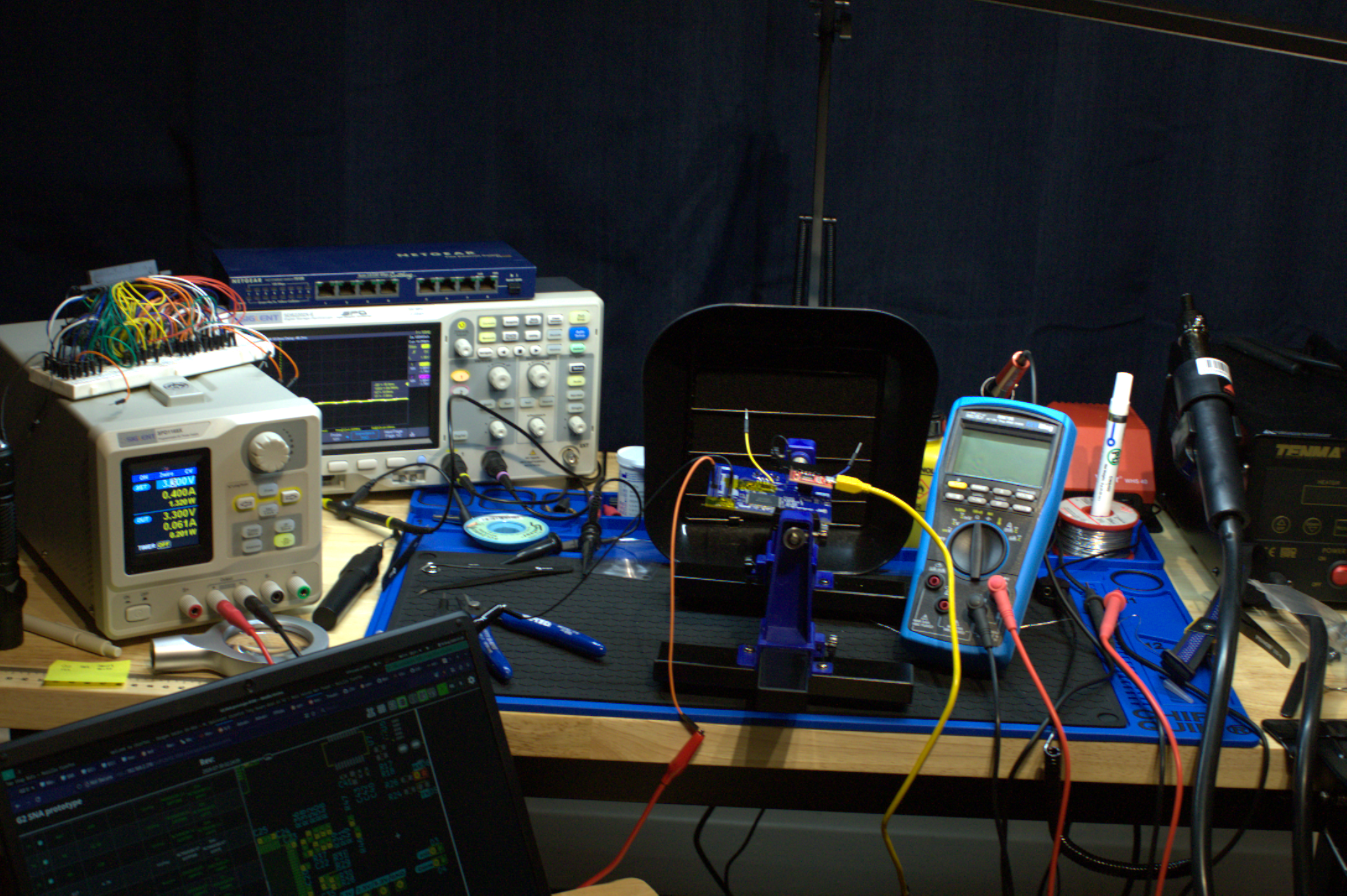
This is the state of my workbench at the time:
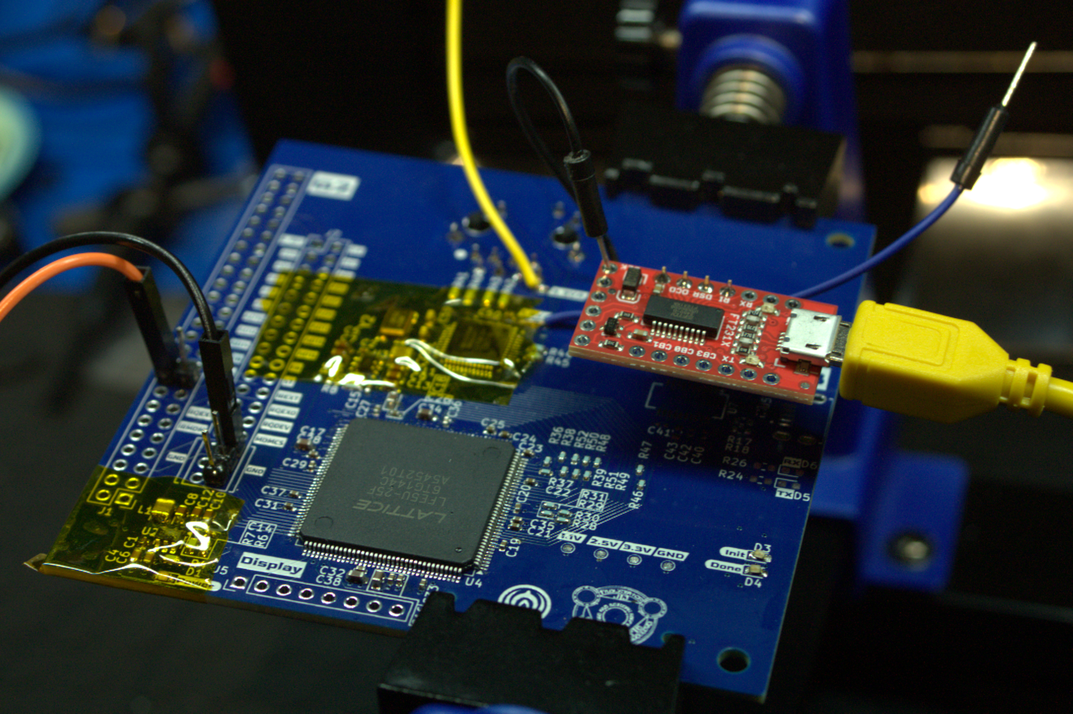
A closer look at the board. I think the silkscreen came out great.
All of this wouldn’t be possible without a whole bunch of hardware and software projects:
KiCad (plus the assorted plugins)
openFPGALoader
ULX3S
Orange Crab
ButterStick
Retro-PETER
After assembly, I could see some things that I need to fix. Mostly in regard to the silkscreen and placement of components. Looking at it under KiCad and then in physical form made it clear that placing the parts as close as possible works well when you don’t consider the assembly process. A mistake I made was not considering the order of component markings. Some of them would go from 1, 2, 3, etc. and others would skip or become mixed up. This is only a bother for components of the same value, such as 0.1uF capacitors.
I’m tempted to remove the USB-based programmer interface, however, as the final unit will need it for end-user programming, I still see it as a good idea to incorporate for testing.
There’s a set of pins exposed for an ePaper display (which will add around £8 to the BOM) that I’ll keep around on this version. It could be used for any SPI-capable display. Much like the Broadband Adapter’s MAC printed on the side, it made me think of using the space on the side for informaiton related to the network statistics and storage available.
In total, the components (minus the display) cost around £48. This cost could be brought down a little by using the non-leaded packages for the Ethernet PHY and FTDI chip (plus it would save some space), but it does compromise on the intended goal of having these able to be hand-soldered without needing a lot of expensive equipment (both for assembly and testing).
I’ve yet to explore what needs to be improved upon further with this board from a functional standpoint. Overall, I’m satisfied with the current state of it. Next comes the hard part of proving that it works as intended. I plan on getting something to output on the display pins, then talk to the Ethernet PHY. After that, I’d like to connect it to a Dreamcast and have it communicate with the TF card.