First practical PCB
It’s far too quiet around here.
I had intended to design a usable PCB after realising that the clock domain crossing (or lack thereof) was incorrect. All of Autumn and Winter was spent working on Shambler, mostly tools. In late January and early February, I wrote a tool to convert the Ninja models from an early Katana SDK into glTF, which I still need to commit the source code for. From April to early June, I had an itch to reverse engineer the European version of Resident Evil for the GameCube. There’s a lot left to do with that, which I may return to this year depending on how far I get with this hardware project.
This is the first real PCB I’ve designed. I’m deciding if it makes sense to embed the logic analyser from Gusman by chaining two RP2350’s together. For the time being, I think that breaking out the signals and relying on an external logic analyser will do.
I can’t say for certain if the ~250ps of delay will make a difference between the signals, which is one of the goals of this board. Taking a look at the modem and BBA, it appears that the tracks are of varying length. It may not be an issue at 25MHz. If anything, the mess of wires I currently have will be reduced.
With any luck, and after checking the footprints match the datasheets again, the board should be populated with parts in August. Assumng that nothing blows up when power is applied.
In the meantime, here’s what I’ve been working on for the last month:
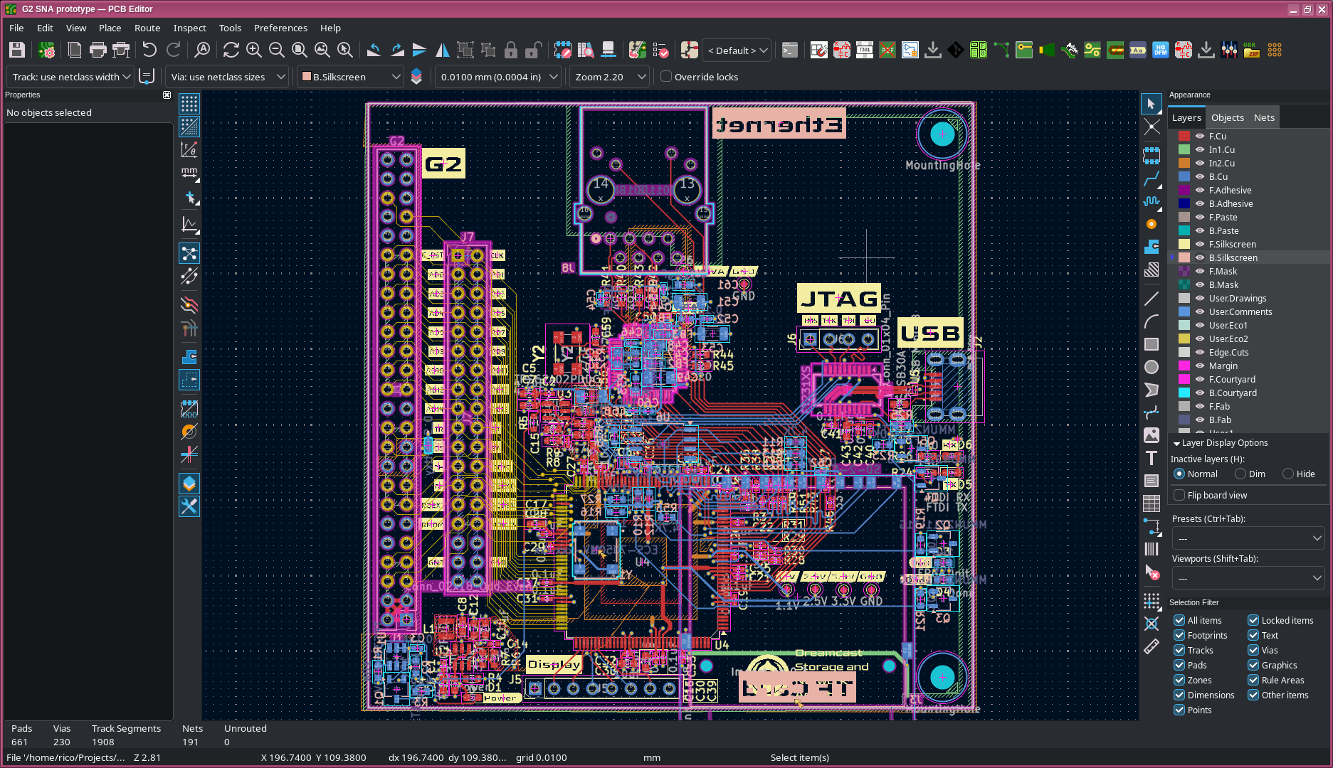
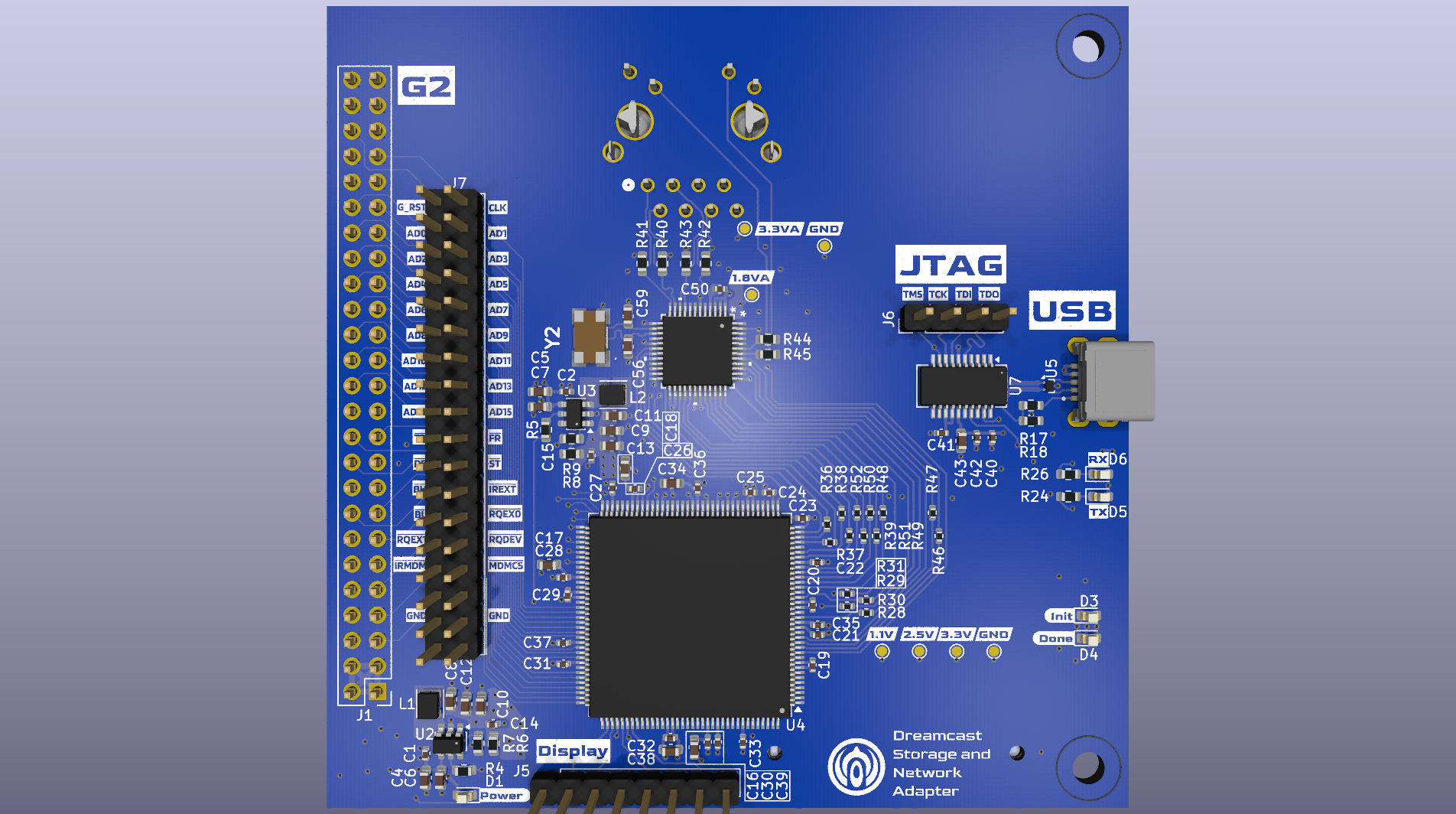
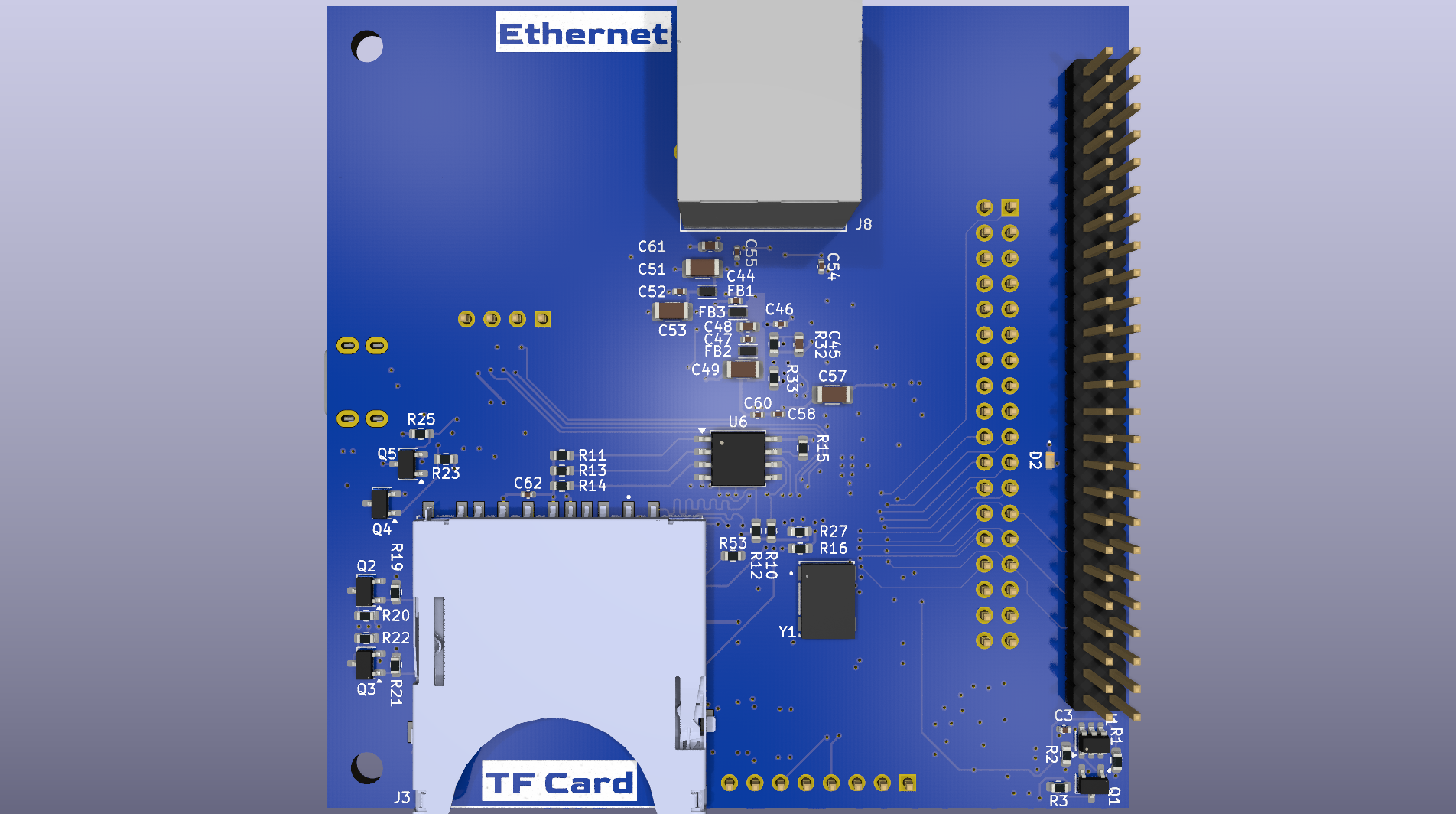
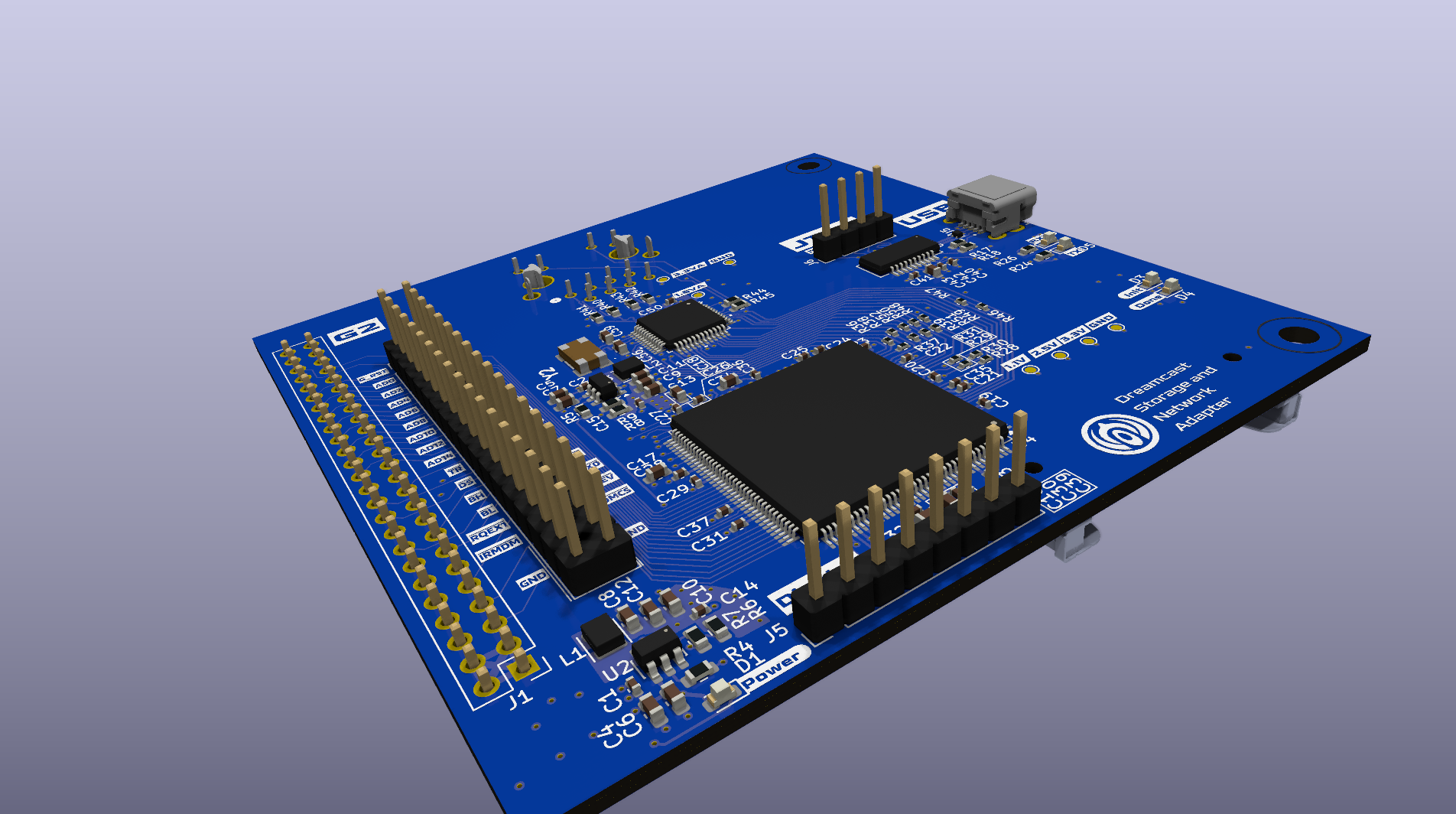
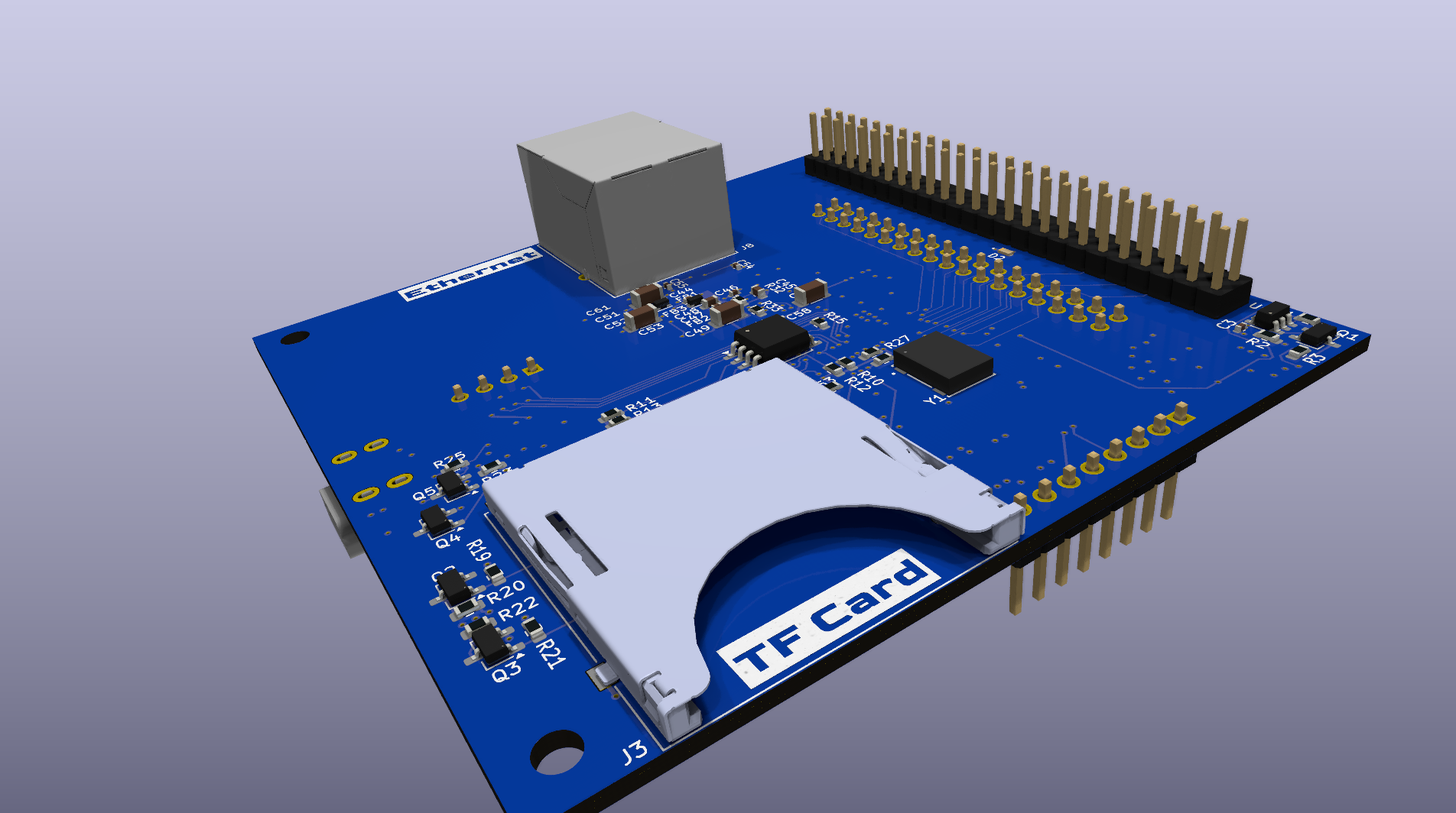
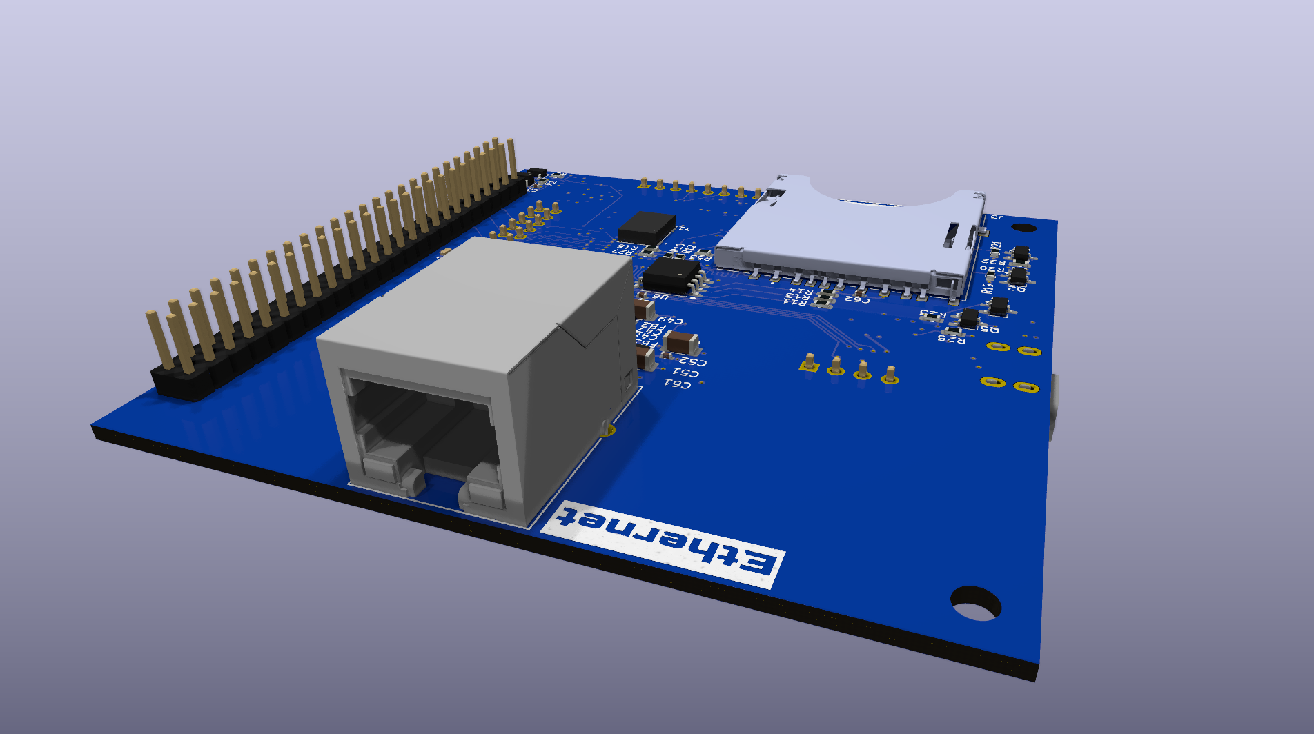
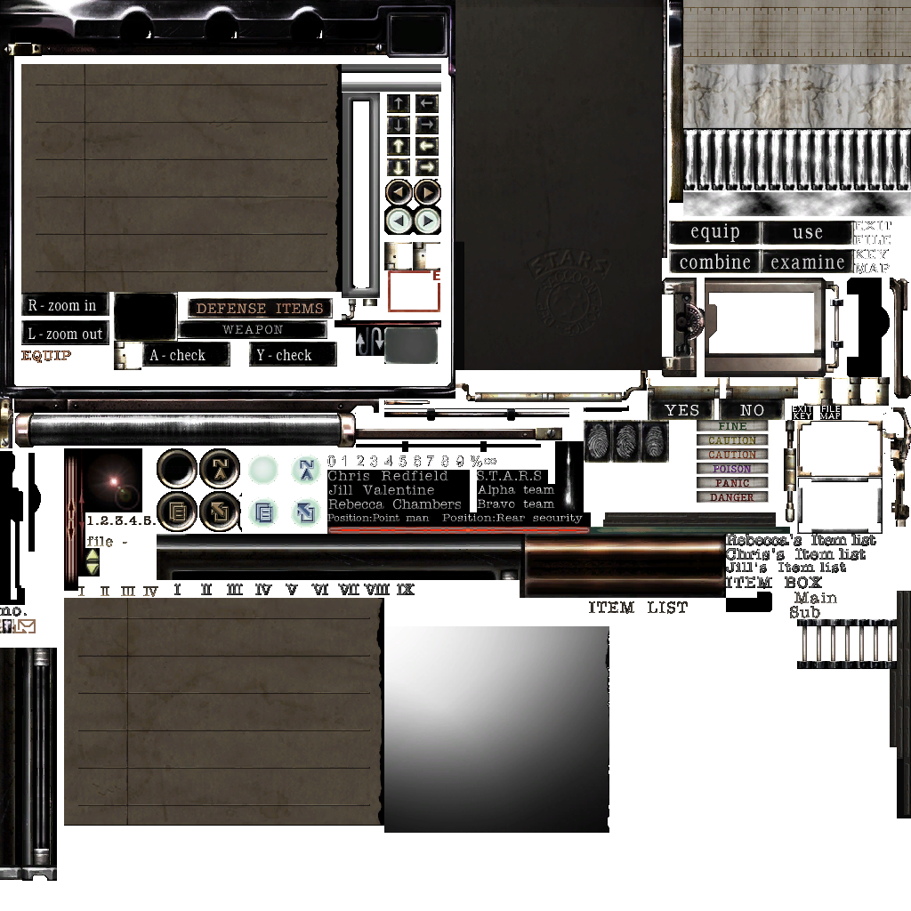
Also, for Resident Evil, I thought that it was interesting how there was an unused Panic status in the inventory screen:
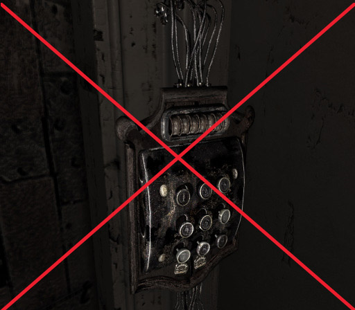
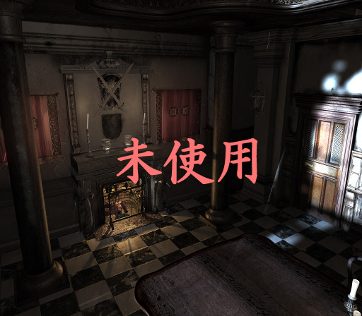
Along with some unused and rejected backgrounds:
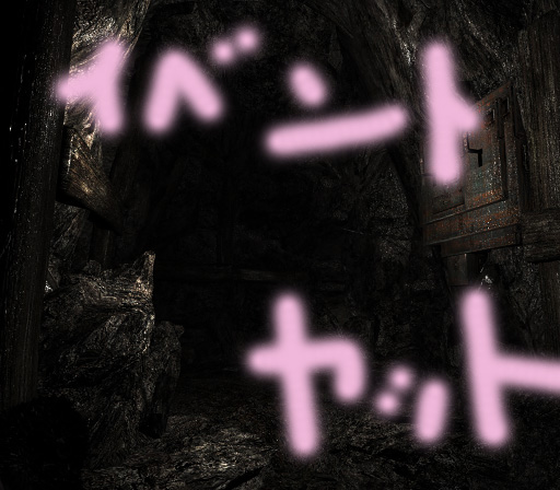
Plus, some image that I have no idea where it’s used:
