Reading and writing NVRAM chips
After waiting a while for the chip programmer, hot air rework adapter for 15mm QFPS, some PLCC32 sockets, and some Kapton tape, I finally managed to take the NVRAM chips off the PortMaster 3 and erase the configuration, keeping the OS intact.
Mostly it consisted of a bunch of waiting around and hours of trying to solder the PLCC32 sockets without needing to snip the plastic in the centre to do it without damaging the socket. I tried two methods to not damage the sockets. The first was to use a fine tip and flow the solder like any other SMD part. I ended up warping the centre plastic and the joints were not great. The second attempt was to wrap the socket up in Kapton tape and hope that it wouldn’t need to be exposed to the hot air for too long before the plastic would start to melt. This wasn’t successful at all and I think the main issue was that I couldn’t see the pins clearly under the tape. It still ended up damaging the socket.
I succumbed with five sockets left and the T1-based PortMaster on the way (with a T1 expansion card, so I can still use the E1 version I already have) that I had to consider for NVRAM socketing. The centre piece of plastic was snipped away carefully (the first attempt ended up with a few clipped pins) for two sockets and set aside to be placed back in later to lift the chip to the height the socket wants it to be at. Then the pads on the board had solder flowed as well as hte pins on the socket. Once that was done, it was a case of lining everything up and soldering it in.
In total, around eight hours was lost due to these failed attempts. It took about 20 minutes per socket with the easier method.
Before trying to write to the NVRAM, I read both of them (labelling one inner and one edge) ten times each and verified that the file diffs came back without any messages indicating that one read didn’t match the others. Of course, I wasn’t going to chance a continuity test as the measure of success for the socket installation. The board was put back into the PortMaster 3 and booted. It came back with a message about the NVRAM not matching what was expected. My heart sank. I was about to call it a night but decided to just reboot the machine and it booted back into ComOS. After the feeling of relief subsided, I checked that the !root login was still not using the default password. Looked about the same as before.
After pulling the board out again, I read the two NAND dumps and determined that the inner chip contained partitions 0-3, with the edge chip having 4-7. The AM29F040 has eight segments each, with a total of sixteen, each chip has an identifier for ComOS specifying which section of the partition it is (0,0 and 0,1 make up the first partition). The documentation mentioned that the configuration is stored on the third partition (partition number 2). Jumping to the offset, I found a string “config” which seemed to be the filename, preceeded by the length of the data and followed by the contents. No quick visible password in sight, I decided to write 0xFF to both partitions 2,0 and 2,1. After writing, the chips were promptly snapped back into their sockets and the board slid into the PortMaster 3.
The login prompt appears and I type !root followed by the default password.
It works.
I’m incredibly relieved that it was as straightforward as it was. The unit still can’t be used in the network as-is, but that’s all right. A T1 board is on the way and due to be here sometime next month. I guess I’ll have to talk about the game instead of the network setup next time.
Below are some of the failed PLCC32 sockets.
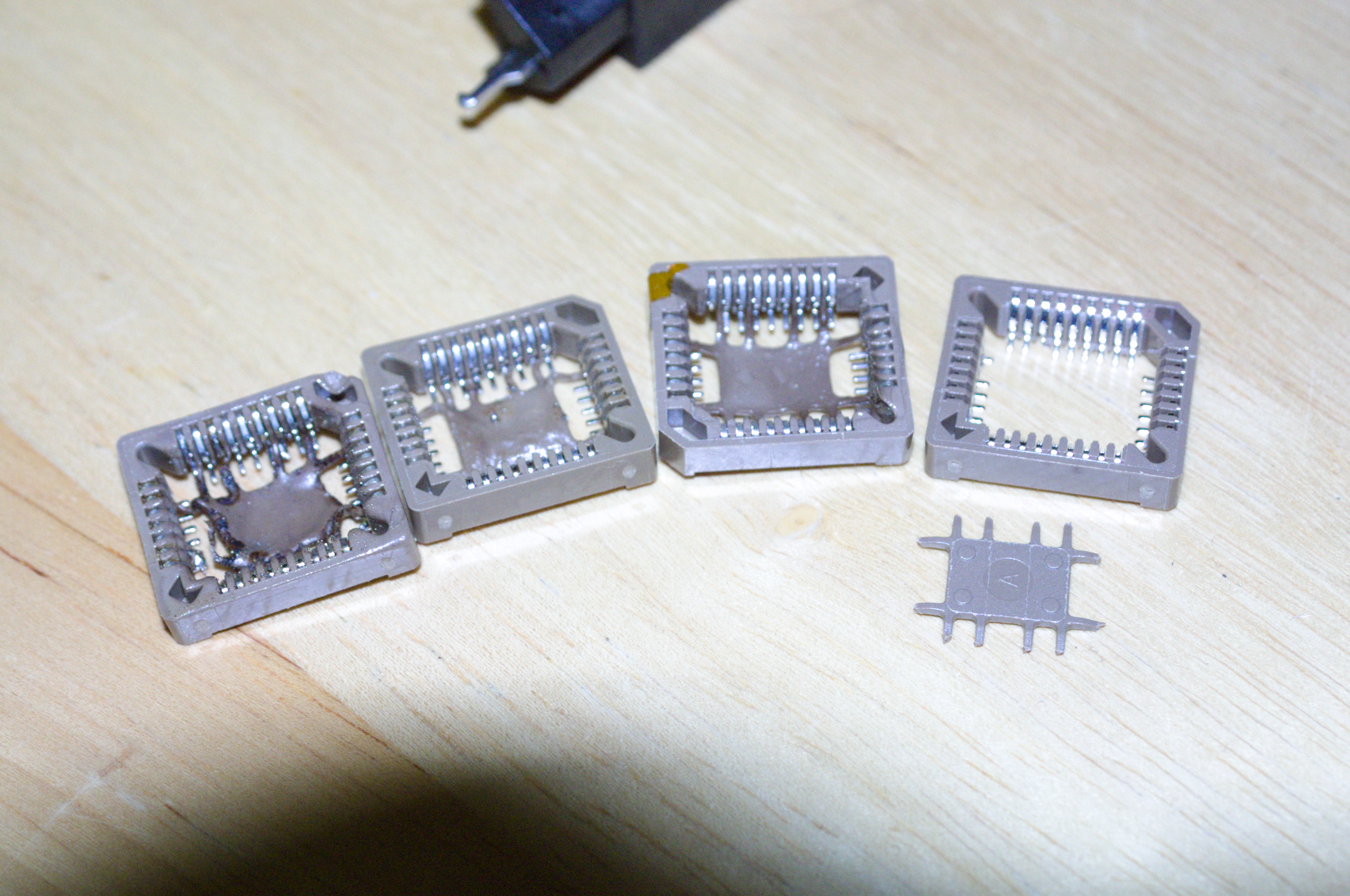
From left-to-right: Two failed sockets from attempting to solder them onto the board without cutting out the centre platform, one which failed with the Kapton tape method, lastly, the one which I got too close to the legs with the side-cutters.